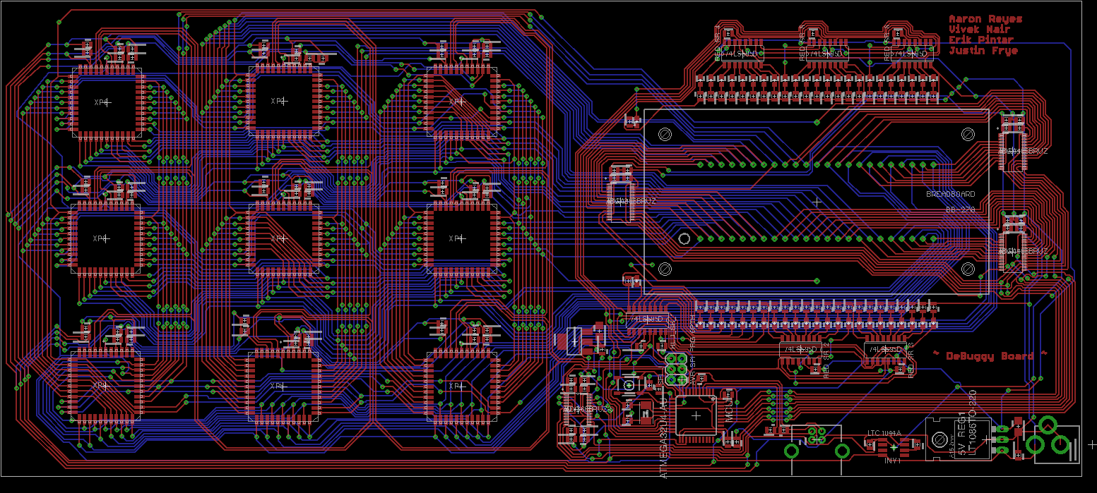
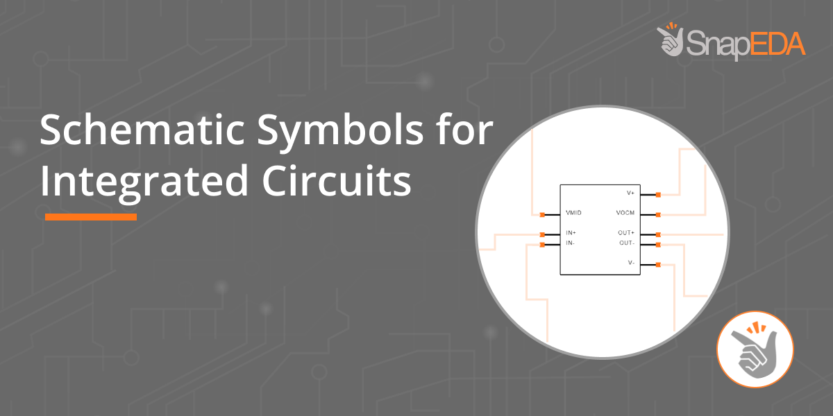
Pin naming, pin setting, and pin arrangement are the 3 most important factors to consider when creating the schematic symbol for an IC device. Considering these aspects will help you create a direct and functional design. At SnapEDA, we developed our own internal standards based on these 3 factors. PIN NAMING To avoid incorrect pin…
-

Track your favorite electronic components with new private libraries!
Read moreYou can now create a free, private library of your most-used electronic components on SnapEDA. After creating the library, you can then download all the symbols & PCB footprints as a single library for easy import into your design tool of choice, rather than downloading each part individually. This quick tutorial will show you how to create your…
-

Easier Ways to Request Symbols & Footprints!
Read moreIt is now easier than ever to request a symbol & footprint on SnapEDA. We also have two new options that deliver the parts into your inbox within 24 hours so you can focus on design optimization, or even taking on new projects. Let’s explore various options for how to request parts on SnapEDA.
-

Introducing the SnapEDA EAGLE Plugin: Find Symbols and Footprints From Within EAGLE (Alpha Release)!
Read moreWhen we initially launched SnapEDA, the goal was to make it as easy as possible for engineers to find CAD models (PCB footprints, schematic symbols, 3D models) for their electronic design tool of choice, in a way that provided them with unprecedented transparency into standards and quality. Our vision was to give engineers the freedom to innovate and optimize their designs, with…

