
Schematic Symbols for Integrated Circuits
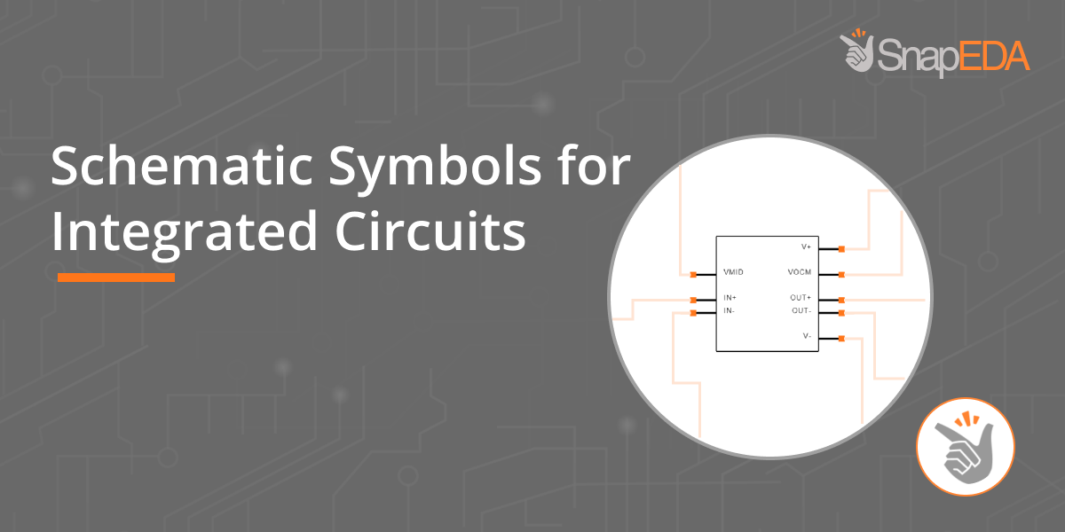
Pin naming, pin setting, and pin arrangement are the 3 most important factors to consider when creating the schematic symbol for an IC device. Considering these aspects will help you create a direct and functional design.
At SnapEDA, we developed our own internal standards based on these 3 factors.
PIN NAMING
To avoid incorrect pin mapping and unwanted connections, make sure to name your pins based on the information available in the datasheet. We recommend adding the names of the alternate functions per pin. However, if there are too many functions and you prefer a more compact symbol, you may use the main pin names.
PIN SETTING
Set the electrical type or direction of the pin. Some of the most commonly used settings are I/O, Input, Output, Power, Passive, Power, and others.
Note that if pins are not properly defined, the earnings response coefficient (ERC) may not work as expected. For further insights, see the examples below:
- Power pins like VCC or Ground = Power.
- Reserved pins or shield pins = Passive.
- NC pin = Not Connected.
- P0.0, P0.1, P0.2 = Input/Output or Bidirectional.
- Chip Select pin = Input.
Additionally, you should always set the pin functionality. This is known as the “graphic style” in KiCad or the “symbol pin” in Altium Designer. It allows you to add the electrical characteristics of a pin, like Clock, Inverted Clock, Input Low, Active Low, and more.
Note: This is not recommended for pins with multiple functions (GPIO3/SCLK/INT/DO).
PIN ARRANGEMENT
The pin direction is an important element to consider when arranging your pins. Based on our internal standard we recommend arranging with these positions:
- Place Input pins at the left.
- Place Output pins at the right.
- Place I/O pins at the middle left (if there are too many I/O pins, place some at the middle right).
- Control pins can be placed at the upper left.
- VCC or power pins are placed at the upper right.
- Place GND pins at the lower right.
- Place NC/DNC pins at the lower left
Another important considerations when arranging pins are the function of the device and the function of each pin. Understanding the behavior of the device and arranging pins in a logical way will allow you to have an operative symbol for your schematic diagram.
The pin functions are available in the pin description, the circuit diagram, or the function diagram.
OTHER TIPS
- If your symbol has +100 pins, separate the symbol into multiple sections based on functionality (PartName_Power, PartName_I2C, etc). This will make it easier to locate the pins when designing your circuit.
- If exposed pads or thermal pads are present, add an EXP pin for an option to connect it to ground.

