
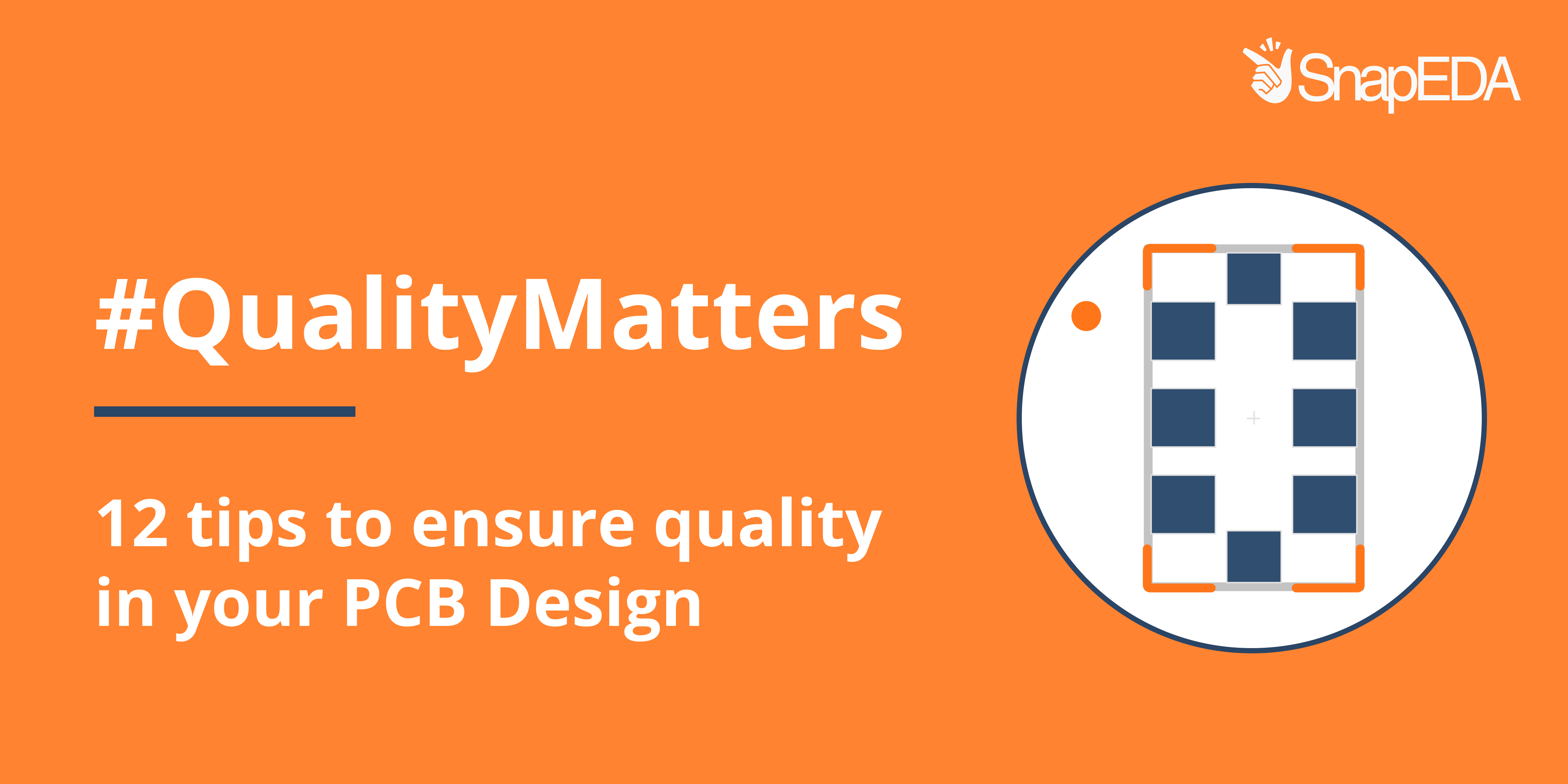
Quality Matters: 12 tips to ensure quality in your PCB Design
At SnapEDA, we aim to provide high quality ready-to-use symbols and footprints for your electronic components. Accurate and well designed libraries for your PCBs are essential for optimal performance of your board. A single error or the slightest offset from a badly created footprint can cause thousands of dollars in wasted prototypes, along with weeks of delays.
Here is the round-up of the 12 tips to keep in mind while designing symbols and footprints for your PCB:
- Tip #1: Add a pin 1 indicator:
Tip: A pin 1 indicator is a small element added to the land pattern. It allows engineers to easily locate the 1st pin to ensure proper orientation before mounting.
— SnapEDA (@SnapEDA) June 1, 2022
At SnapEDA, we ensure all relevant land patterns contain an indicator! #QualityMatters #PCBDesign #Electronics pic.twitter.com/ElA9jp6yYp
- Tip #2: Keep a 0.25mm silkscreen to pad clearance:
#QualityMatters Tip #2: Silkscreen on exposed copper areas can prevent a good flow during the soldering process. Based on IPC guidelines for land patterns, at SnapEDA we add a 0.25mm silkscreen to pad clearance.
— SnapEDA (@SnapEDA) June 6, 2022
Start exploring: https://t.co/R3zWLworjk
#PCBDesign #Electronics pic.twitter.com/ZrfMg3AJS5
- Tip #3: Arrange pins based on function and electrical type:
Tip #3: Proper pin arrangements and correct pin directions are the 2 main factors in creating your schematic symbol. At SnapEDA, we arrange the pins based on their functions and electrical type.
— SnapEDA (@SnapEDA) June 13, 2022
Start exploring at https://t.co/SZ5oXjp76O#QualityMatters #PCBDesign #Electronics pic.twitter.com/Ly8RjU0UIa
- Tip #4: Use standard schematic symbols:
Tip #4: Use standard schematic symbols for good representation of the components in your diagram and to easily understand the flow of the circuit. @SnapEDA provides schematic symbols based on IEEE standards that are used by engineers worldwide.
— SnapEDA (@SnapEDA) June 22, 2022
Check out https://t.co/R3zWLwoZ8S pic.twitter.com/xknUQy81Mt
- Tip #5: Follow manufacturer’s recommended land pattern:
#QualityMatters Tip #5: While it is important to follow standards, it is also essential to consider manufacturer recommendations for some packages. Creating custom land patterns can improve the device’s thermal performance. Start exploring at https://t.co/yQyMzNIcOn pic.twitter.com/YRonZtNjWd
— SnapEDA (@SnapEDA) June 28, 2022
- Tip #6: Use the exact shape for slotted holes:
#QualityMatters Tip #6: At SnapEDA, we don’t just create plated through-hole patterns with the correct drill diameter, we create the exact shape for slotted holes as well. We provide accurate CAD models.
— SnapEDA (@SnapEDA) July 6, 2022
Learn more: https://t.co/WUW4T3hJMf#slottedholes #electronics #pcbdesign pic.twitter.com/q7T77eePcr
- Tip #7: Manual vs Automated models:
#QualityMatters Tip #7: Manually-created CAD models are perceived to be preferable compared to auto-generated ones in terms of quality. However, at @SnapEDA, all automated CAD models were generated based on the libraries our in-house engineers created.https://t.co/JhbvL9XAIV pic.twitter.com/33ugLrHB6X
— SnapEDA (@SnapEDA) July 14, 2022
- Tip #8: Use detailed connector symbols:
#QualityMatters Tip #8: Using detailed connector symbols is preferable because it allows you to quickly identify whether you’re using a male header, a female receptacle, a jack connector, and many more😀.
— SnapEDA (@SnapEDA) July 27, 2022
Start exploring at 👉 https://t.co/R3zWLwG2aS. #pcbdesign #electronics pic.twitter.com/Zz9Rgk09yV
- Tip #9: Add details to your schematic symbols:
#QualityMatters Tip #9: Missing details in your schematic symbol can lead to misinterpretation of the device, which could affect the connections in your circuit design.
— SnapEDA (@SnapEDA) August 4, 2022
Check out SnapEDA to download accurate, detailed schematic symbols. 👉 https://t.co/R3zWLwG2aS pic.twitter.com/vzN15ATUku
- Tip #10: Use standard pinout configurations for USB connectors:
#QualityMatters Tip #10: It’s better to use a schematic symbol with specific pin names, following the correct pin descriptions, to easily connect the pins in your circuit design 🙂
— SnapEDA (@SnapEDA) August 12, 2022
Start exploring at 👉 https://t.co/R3zWLwG2aS.#qualitymatters #PCBDesign #Electronics pic.twitter.com/X8iPNGZBi6
- Tip #11: Use segmented solder paste for thermal pads:
#QualityMatters Tip #11: Using segmented solder paste for thermal pads with over 4 mm² of land area is recommended. Too much solder can cause component shifting, and segmented solder paste can help avoid this defect. 😀
— SnapEDA (@SnapEDA) September 9, 2022
Start exploring at 👉 https://t.co/R3zWLwoZ8S. pic.twitter.com/S9cMJUucqO
- Tip #12: Add restricted areas for high signal sensitivity devices:
#QualityMatters Tip #12: It is recommended to add restricted areas for devices with high signal sensitivity such as transducers or transceivers. Adding restricted layers to the footprint ensures uninterrupted signals in your circuit design.🙌
— SnapEDA (@SnapEDA) September 19, 2022
👉https://t.co/R3zWLwoZ8S pic.twitter.com/cDkabl0j2G
We hope you found these tips helpful when designing your PCB board. Make sure to follow these to ensure high quality and performance for your device.
Happy designing!


Comments (4)
Daniel Lacerda
February 10, 2023 at 3:52 am
Hey Daniel Lacerda here !
That’s awesome !
Great and important tips !
Faust Arenas
February 10, 2023 at 9:12 am
Hi Daniel,
We’re glad you liked it.
Please let us know if you have any questions regarding design and SnapEDA. We’re here to assist you.
ha7vc
February 16, 2023 at 9:45 pm
Hi,
Congratulations for the team!
Best regards,
Laci.
ERP Software
April 5, 2023 at 8:25 pm
That’s very interesting and informative tips on ensuring quality standards in pcb. Thanks for the article.