
Helping engineers select and design-in electronic components with Seeed
Today we’re announcing a new collaboration with Seeed, a global PCB manufacturer, and creator of the Seeed and SheZhen open parts libraries (OPLs).
The OPLs are a collection of commonly used components used in printed circuit boards (PCBs), designed to be used with the Seeed Fusion PCB Assembly service. By using these components when designing, engineers can speed up production and lower costs, since the components are more likely to be in stock, and are purchased in bulk to maximize cost savings.
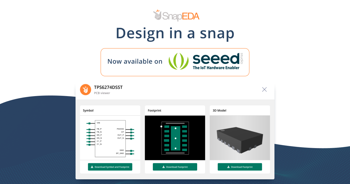
We are thrilled to announce that we will be supporting Seeed’s efforts by enriching the OPLs with SnapEDA’s CAD models. Engineers can now find SnapEDA’s ready-to-use computer-aided design (CAD) models within Seeed’s open libraries (OPLs) to help them move from idea to production seamlessly.
Engineers at the component selection stage face 3 key challenges: :
1. Stock and availability: Is the component available in the supply chain? Given the current semiconductor shortage, this question has become more pressing than ever.
2. CAD model availability: Do the parts have symbols, footprints and 3D models available? If the answer is no, they would need to create them from scratch, which could represent hours or even days of time.
3. Cost: Does the component selected optimize the bill of materials (BOM) cost?
Seeed’s OPLs solve these problems with its curated collection of 150,000 parts selected on the basis of being widely available and cost effective.
With the new SnapEDA integration, engineers will be able to solve the most time-consuming barrier of all – finding CAD models for their designs.
The SnapEDA models are available in over 15 PCB design formats such as Altium, Autodesk EAGLE & Fusion 360, Cadence OrCAD & Allegro, and KiCad.
How to find and download SnapEDA models on Seeed
1. Go to www.seeedstudio.com/opl.html
2. Click either in the Seeed OPL tab or the ShenZhen OPL tab.
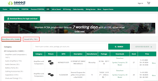
3. Search for the part you need
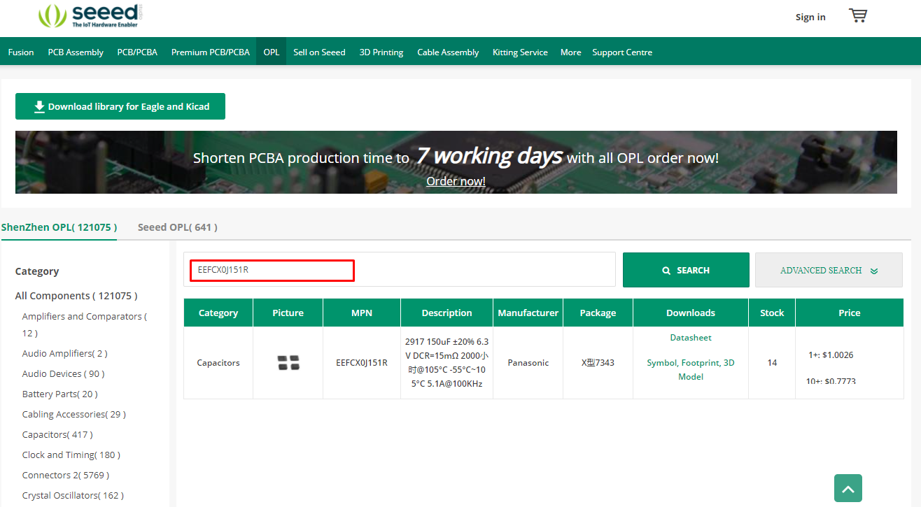
4. In the download’s section, click the Symbol, Footprint and 3D model link
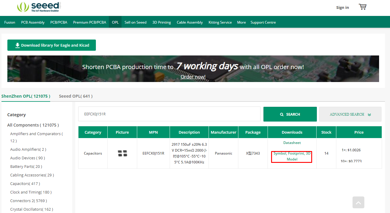
5. A viewer will popup allowing engineers to preview the models, and download instantly.
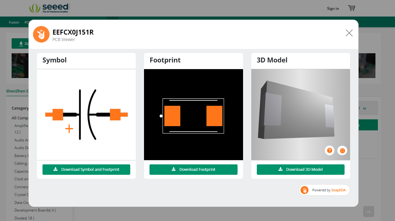
6. Click Download to get the CAD models (symbol, footprint, 3D models) and export them to your PCB design tool.
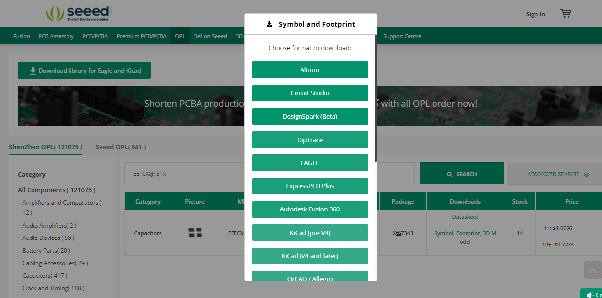
And that’s it! The CAD model will download instantly for use in your PCB design tool.
Happy designing!