What are QFN Packages?
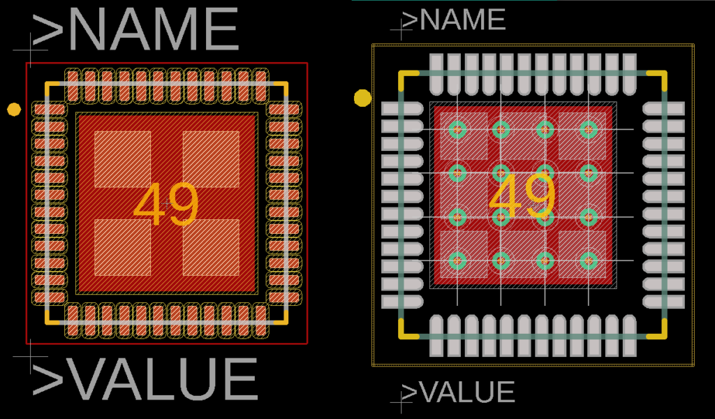
QFN (quad flat no-lead) package is an IC component best used for programmable modules and microcomputers. It is also recommended to use this package for PCB designs with size, thickness and weight considerations. It is also known as quad micro leadframe package.
Using QFN Packages
Pros:
- Size and weight
– It is a thin, compact package that occupies lesser surface area ideal for any PCB design. It is also very light, which is applicable for boards with thinner material - Thermal dissipation
– It contains an exposed pad to improve the chip’s thermal performance or heat distribution - Low cost
– Various manufacturers are producing QFN packages nowadays which makes the cost cheaper. It is also inexpensive to manufacture PCBs with QFN packages since the assembly requires lesser time and materials for mounting
Cons:
- Soldering
– There is a higher risk of solder-bridging due to its narrow pad-to-pad pitch. Since it’s a no-lead package, it would also be a challenge to desolder when needed.
Kinds of QFN Packages
QFN with tab vs. QFN with no tab
Some users prefer a QFN package with no thermal pad to avoid the possibility of solder overflow and solder bridging. However, the most common QFN package contains a thermal pad in the center of the device for better thermal distribution. Solder bridging can be avoided by making sure the solder paste in your exposed pad is segmented. It is recommended that the solder paste only occupies 40% of the thermal pad’s area.
Pull-back QFN
This kind of QFN package has pullback metal pads from the edge of the component’s body, the terminals are not visible once mounted.
QFN with wettable flanks
QFN with wettable flanks has an elevation that shows solder wetting. This enables the designer or manufacturer to visually inspect and ensure each pad is mounted to the board.
Wire bond or Flip chip QFN
Wire bonding and flip chip bonding are two assembly methods to mount a kind of QFN package with active areas or pads located at the top of the chip. The wire bonding method uses wires to connect the chip’s terminals directly to other semiconductors, integrated circuits or PCB tracks. For flip chip bonding, the chip is flipped facing downwards to directly mount it to the board. The chip’s terminals are connected to the board with solder bumps that were deposited on the pads.
How do we create QFN land patterns at SnapEDA?
At SnapEDA, we always create our QFN land patterns based on IPC standards. However, our engineers also analyze and consider the paste stencil and thermal via patterns recommended by the manufacturer to provide users with land patterns that offer the best design for improved thermal performance.