
What are anti-pads, and how to create them in Eagle
What is an anti-pad?
An anti-pad refers to the area around a plated through-hole, which voids or restricts other signal traces that should not be connected to that particular through-hole. They are often added to avoid short-circuits between neighboring holes.
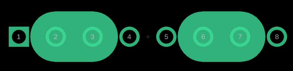
How do we add anti-pads in Eagle? The only way to form a layout closer to an actual anti-pad in Eagle is by adding all restrict layers (tRestrict, bRestrict, vRestrict) around the plated through-hole. The only limitation with this method is it only restricts traces within the top and bottom layers, it does not add restrictions for internal PCB layers. Below is a simple graphic demonstration on how to draw an anti-pad in Eagle.
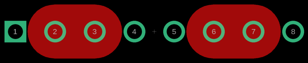
- Using the Polygon tool, create the shape of your anti-pad in tRestrict layer (top layer).
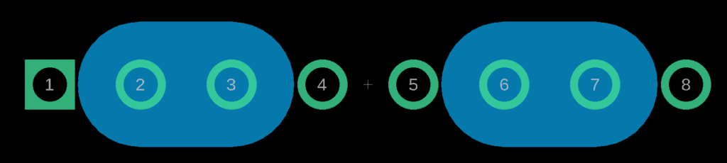
- Copy the created anti-pad in tRestrict layer and you now have a 2nd anti-pad. Make sure to change the layer of the 2nd anti-pad and set it to bRestrict (bottom layer).
- Copy another one to have a 3rd anti-pad and set it to vRestrict layer (via layer).