

What is a Solder Paste?
A Solder Paste, also known as Solder Cream, is a material used for mounting and soldering components to printed circuit boards. It is used in reflow soldering commonly for surface mount devices but it can also be used for through-hole components (pin-in-paste).
The paste consists of flux and powder solder. The powder solder are tiny solder balls that are suspended in the flux. It comes in different micro sizes and it is composed of lead paired with a metal element such as tin, silver or copper. The flux is an agent that carries the solder balls and it temporarily holds the components in place for soldering.
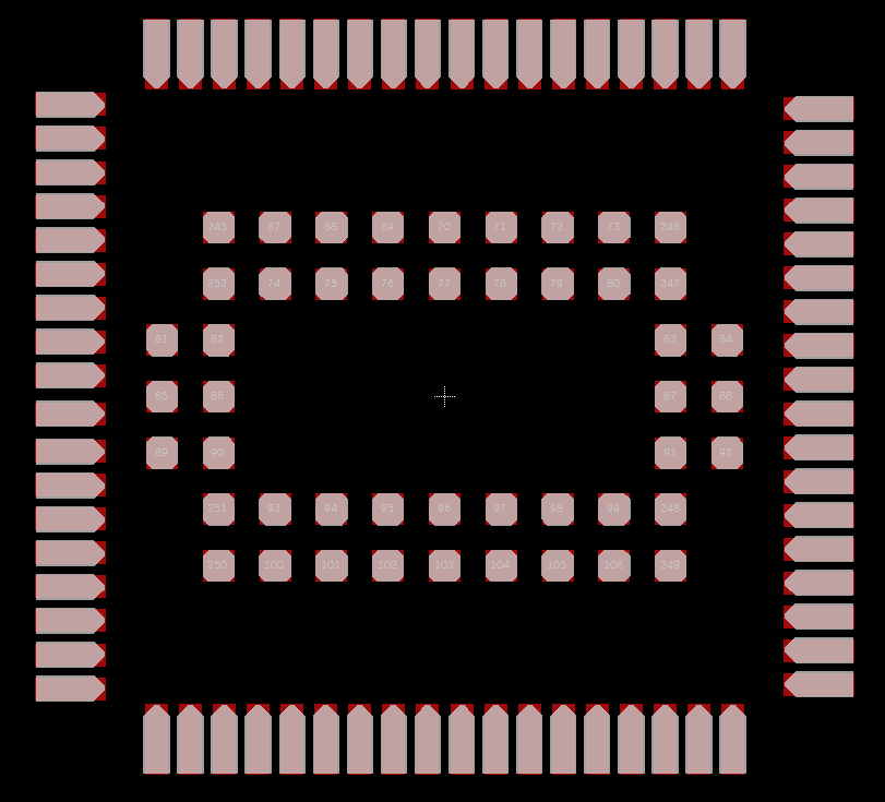
The process of adding solder paste begins with the paste mask stencil. The stencil is a thin metal sheet with slotted patterns. It is placed against the board (the stencil should be aligned with the copper pads) and the solder paste is applied all over. The stencil is then removed and the components can now be mounted temporarily to the board. The board will undergo a heating process which will melt the solder balls in the paste and will permanently bind the components to the board.
When creating a land pattern for the components, a cream or paste mask layer must be present for the stencil design. The standard paste mask size is equal to the value of the pad size. However, some components with narrow lead pitches are recommended to have smaller stencil sizes or offset stencil pattern for better soldering and to avoid solder bridging.

In terms of thermal pads or exposed pads, SnapEDA follows IPC-7351B paste mask standards. It is recommended to set the size of the paste mask to only 40% of the whole pad area for thermal pads 4.0 mm or less.

It is also advisable to create the stencil design as segmented squares or rectangles instead of just 1 whole paste area for thermal pads, this applies to pads with land area over 4.0 mm. This design recommendation enables the component to settle to the pad better, rather than floating on top of the solder paste.

At the end, either the printed board assembler or the designer can modify the information provided for openings in the stencil in order to meet specific solder volume requirements, see IPC-7525 for more information.