

What is a Solder Mask?
A Solder Mask (solder resist) is a protective layer applied to your PCB, generally applied on the top of the copper traces, to avoid short circuits due to solder shorting or solder bridging between components. PCB solder resist also gives additional protection to the board, preventing it from corrosion or any harmful environmental agents.
The process of applying solder mask to your PCB is usually done in fabrication industries (although, there are a lot of kits available for Do-It-Yourself circuit boards) and there are different kinds of solder masks, it comes in dry film, liquid ink or liquid epoxy. The commonly used material is the dry-film photoimageable solder mask. The board will undergo film lamination and the PCB pattern will be exposed to the laminated board under a UV light. A developer solution is then used to wash out the unwanted resist areas.
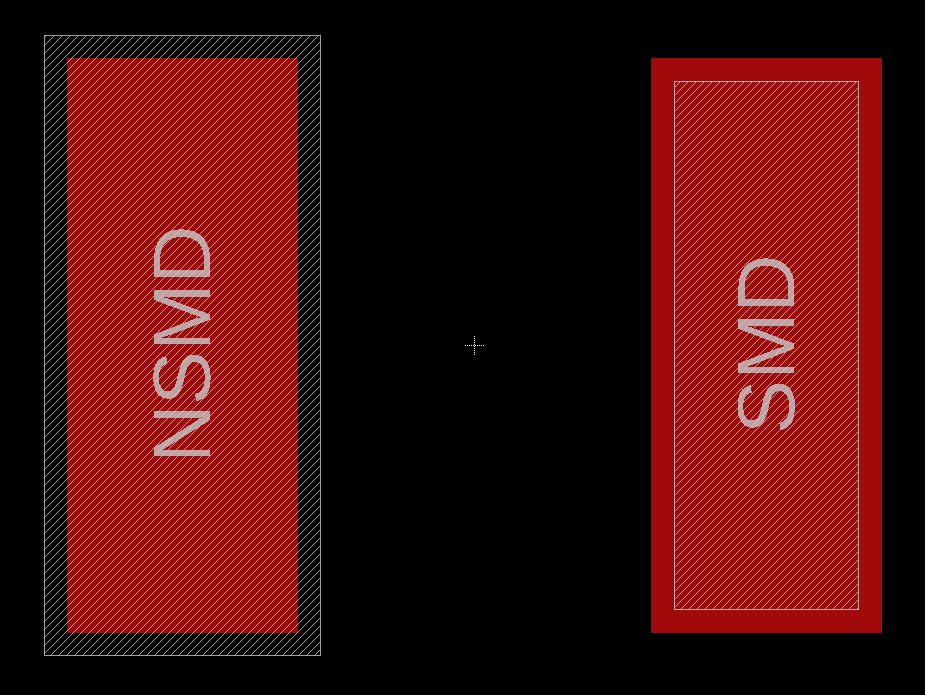
Non-Solder Mask Defined vs. Solder Mask Defined Patterns
Most PCB land are copper-defined or non-solder mask defined (NSMD). Usually, non-solder mask defined pads have solder mask openings larger than the copper land pads. NSMD patterns provide a bigger soldering surface area and a good clearance between pads.
Solder mask defined (SMD) patterns, on the other hand, have solder mask openings smaller than the copper pads. This method is usually applied when the component has a narrow pitch. Since the solder mask opening is smaller, it reduces the surface area of the pad preventing the solder to smudge to the next pad.
It is highly important to choose the correct solder mask window for your land patterns, if there are routed conductors between your lands, the solder mask should cover the conductor, this type of solder mask window is known as pocket solder mask or you can design a gang solder mask window if there are no conductors running between your PCB lands.
For best practices, and if you want to follow IPC-7351B recommendations, your solder mask openings should be 1:1 scale of the pad size allowing your manufacturer to easily modify your land patterns to match their board fabrication tolerances. Many manufacturers recommend solder mask openings should be approximately 2-3mils per side larger than the pads and the default design rules in some EDA tools check for a minimum solder mask opening of 4mils per side larger than the copper pads.