

Understanding Through Hole Land Patterns
What is a punched hole? Should I use the drilled hole diameter or the finished hole diameter? I bet you’re thinking of those questions when trying to create your PCB land pattern for a through-hole component.
At SnapEDA, our engineers analyzed different through-hole land patterns to help you produce the best libraries for your designs. Here’s a guide to help you design a through-hole land pattern.
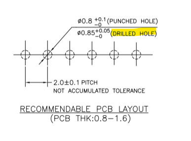
Drilled Hole vs. Punched Hole
Some land patterns suggest 2 hole diameters: the punched hole diameter and the drilled hole diameter. These diameters are the recommended sizes to follow based on the the kind of hole-formation method used during manufacturing.
The names themselves basically explain the method. Drilled holes are formed by loading a drill bit to a cutting/drilling machine or a mini hand drill. Punched holes are formed by using a die set and putting pressure to the board using a punching machine. Although it is easier to produce holes in different shapes using the punching method, the commonly used method is the drilling method. The drilling method has a faster processing time and it is more applicable and flexible to use for different kinds of boards.
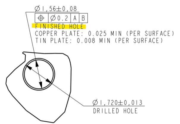
Finished Hole vs. Drilled Hole
Most land patterns only state the recommended drilled hole diameter but there are instances when the datasheet states a finished hole diameter as well. If the finished hole diameter is given, we recommend selecting this hole size instead of the drilled hole diameter. When given these 2 options in the land pattern, the drilled hole size refers to the drill bit size recommended for manufacturing. The finished hole diameter is the recommended hole size for your PCB land pattern – it’s the reduced size when the through-hole is plated. Board manufacturing industries also prefer to get the finished hole diameter and they’ll be able to determine which drill bit to use.
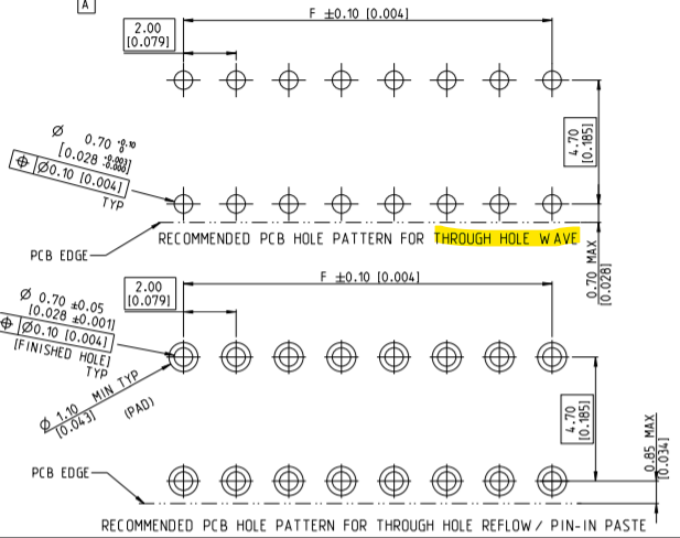
Through Hole Wave vs. Through Hole Reflow
There are datasheets that offer 2 recommended PCB hole land patterns based on the mounting methods, one for Through Hole Wave soldering and another for Through Hole Reflow or the Pin-In-Paste method. To select your hole pattern, you should first understand the mounting method you’ll be using. Through hole reflow uses a pin-paste or paste-in-hole technology wherein a solder paste layer and stencil is added to your through-hole design. The board with the solder paste is then being heated and the solder reflows to the terminal. After the heating process and once it cools down, your component is now mounted to the board. Through hole wave soldering is a more common mounting method for through hole components. The components are glued to the board, solder flux is sprayed to it and it passes through a heating machine where the solder melts and forms a wave which bonds the components to the board.
Comments (2)
Joe Bak
October 2, 2020 at 4:47 pm
Your description of wave soldering is not quite correct.
The “wave” is wave soldering is a molten pool of solder that is pumped through an elongated nozzle that covers the entire width of the PCB. The PCB is put on a conveyor that moves the PCB through a preheater, then a sprayer that applies flux to the bottom (solder) side of the board, and finally across the molten wave of solder. The solder adheres to the exposed leads and pads on the bottom of the PCB, forming solder joints.
Gluing is not required for through-hole mount components that are placed on the top (component) side of the PCB. Gluing IS required for surface mount technology (SMT) components that are placed on the solder side of the PCB. SMT components that are wave soldered must be able to withstand the thermal shock of being dragged through molten solder. These SMT components must also have widely spaced terminals (coarse pitch) to avoid solder bridges from forming.
There is an additional soldering technique for through-hole mount components called Selective Solder. Instead of a large, linear wave of solder that touches every point on the bottom of the PCB, selective solder has a small “fountain” of solder that is just big enough to solder a single pin (or a small group of pins) at a time. This fountain is moved from pin to pin on the bottom of the PCB by a robotic mechanism, allowing it to avoid fine pitch SMT parts that were soldered to the bottom of the board by a previous reflow operation.
Elizabeth Bustamante
October 5, 2020 at 9:08 pm
Hi Joe. Thanks so much for your comment and for reading this article! We really appreciate your suggestions as well, we will create a different blog post to talk about the process of wave soldering so we can share more details about it. For this article, we were mainly focused on the kind of through-hole pattern to be used based on the soldering method.
We are definitely editing this blog post to include the technique you mentioned (selective solder), thanks again for sharing!