

The IPC-7351 Specification Explained: SOIC Components
One of the most common questions designers have while creating printed circuit board (PCB) footprints is: what are the correct dimensions for the pads? Increasingly, designers are adopting the IPC-7351 standard, which provides guidelines for calculating pad dimensions. In general, following standards is a good idea since it helps maintain consistency, accuracy, and reliability — all important things to consider when trying to de-risk your designs, reduce prototype iterations, and get things right the first time.
In this article we’ll be exploring how the IPC standard is applied to small outline integrated circuits (SOICs), a popular package type for electronic components. In further blog posts we’ll delve into some of the other types of ICs, including leadless and through-hole packages.
When creating a footprint for a SOIC, it’s important to recognize that they can differ based on the package’s body size, pad span, pitch of leads, and so on. This is why it’s essential to make sure you have an SOIC footprint that matches the exact dimensions and tolerances of the manufacturer’s package for the component you are using. Additionally, there are also other flavours of SOICs, including J-leaded ones.
The IPC-7351 standard requires three important dimensions when calculating the footprint (or land pattern) dimensions for an SOIC: the maximum dimension from pad to pad (L), the inner dimension (s), and the width of the pad (w).
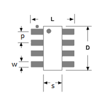
Figure 1: A general SOIC Footprint
The IPC-7351 Equations for SOICs
In order to calculate the pad dimensions, the IPC-7351 specifies three main equations, following the MMC (maximum material condition) environment:
Zmax = Lmin + 2Jt + sqrt(Cl²+F²+P²)
Gmin = Smax – 2Jh – sqrt(Cs²+F²+P²)
Xmax = Wmin + 2Js + sqrt(Cw²+F²+P²)
* The value of L can be derived from the package dimensions. It is the value from lead termination end to lead termination end. W can also be derived from the package dimensions; it is the width of the lead or termination. S is the distance between component terminations, which can be calculated as follows:
Smax = Lmax – 2(Tmin), where T is the lead length as measured across the footprint (also provided from the package dimensions)
* Jt, Jh and Js are solder fillets to the toe, heel and sides
* Cl, Cs and Cw are the component tolerances. The component tolerances are the variations given in the datasheet. For example: L is 0.5 +- 0.2 – thus 0.5 is the nominal dimension and 0.2 is the tolerance Cl.
* F and P are the fabrication and placement tolerance. IPC uses a standard value of 0.1mm for each.
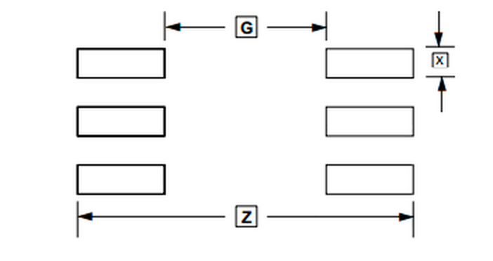 Figure 2. Calculated SOIC Pad Dimensions
The table below shows the values for the solder fillet (Jt, Jh and Js) according to each environment (maximum, median or least).
| Maximum | Median | Least | |
| Jt | 0.55 | 0.35 | 0.15 |
| Jh | 0.45 | 0.35 | 0.25 |
| Js | 0.05 | 0.03 | 0.01 |
Table 1: Values for solder fillet (Jt, Jh, and Js)
Now that we have all the equations, it is easy to check if a footprint downloaded from SnapEDA follows the IPC standard.
In Figure 3, you’ll see an SOIC footprint downloaded from SnapEDA. In this figure, the red rectangles are the pads, while the white layer on the top of the pad is the documentation layer, whose dimensions are the same as the component outline, as specified by the IPC. Also, you’ll notice the silkscreen layer, showing the pin 1 indicator as required.
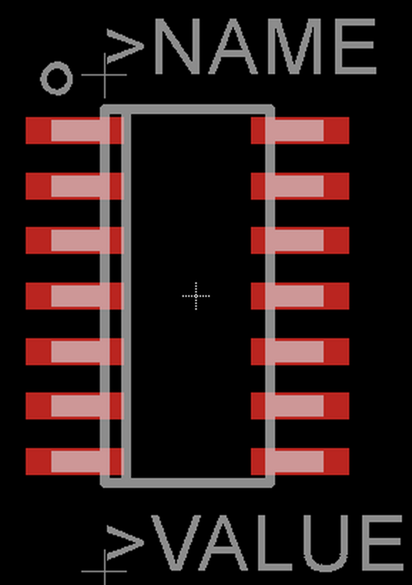
Figure 4: A SOIC PCB Footprint Downloaded from SnapEDA
To summarize, in this post we learned about the IPC industry standard and how they are applied for SOIC packages. The next posts will bring more information about SMD rules for calculating the pad dimensions for other types of components, including leadless packages, and through-hole packages like TO (Transistor Outline) packages.