

How to define cutouts and slotted holes in Eagle (for OshPark users)
Although it’s one of the most popular PCB design tools, Eagle doesn’t have a native way of defining plated slots. Luckily, there are methods of getting fully supported slots in Eagle!
SnapEDA follows Eagle’s official method when defining slotted holes. This method is ideal for 2 layer boards. Please note though that if your board has many layers, and some are internal copper layers, that you’ll need to isolate the slot from them manually to avoid short circuits. Alternatively, you could also create the slots in the dimension layer instead of the milling layer. You can see our FAQ on slotted holes in Eagle here.
If you are uploading your zipped Gerber files to OshPark, you should pay close attention to your slotted holes. OshPark only applies guarantees to slots indicated on the drill layer. Drawing slots on the outline layer usually works, but doesn’t generate guarantees.
So, if, after processing, you don’t see the drill slots in the output files while verifying your design, please re-design your library by following the method described below.
1. Place two vias where the slot starts and ends.
2. Set the drill size of the pad to the desired slot width.
3. Draw a line between the center of each via on the Milling layer using the line tool.
4. The line width must be equal to the desired slot width.
5. Draw two more lines between the via centers on the top and bottom layers.
6. The width of these two lines would be your pad diameter size, but at minimum must be (slot width) + 2*(annular ring).
7. Next, draw two more lines between the via centers on tStop and bStop.
8. The width of these lines should be the same as the copper, or, you can make them up to 4mil (0.1016mm) wider to account for mask expansion.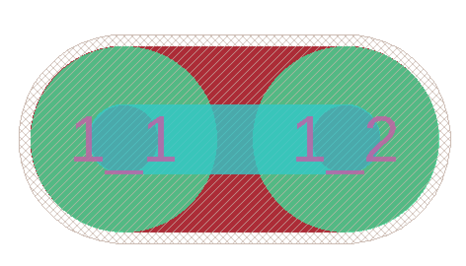
Note: For 4 layer boards, it’s recommended to draw 2 additional lines on the internal layers to connect traces.
According to OshPark, the official recommendation from Eagle works many times, so it’s not required to redo parts. But it’s not guaranteed, just like other outline methods, which is why it’s always a good idea to double check.
There are many ways to draw slots in Eagle. The most important thing is to make sure that your PCB manufacturer is interpreting them correctly, and that the file is correctly defining the slot size, shape, and location for your particular design!
Happy designing!


Comments (3)
Zorgloub
March 17, 2022 at 10:08 am
Your explanation speaks sometimes of vias, sometimes of pads!?
It’s not very clear!
Either you use one or the other… for the same explanation!
User of an “old version” of Eagle, one cannot integrate vias in the libraries.
So, if you want to create, in a library, such a component with a slot you will have to use pads.
On a board, you can always use this method with vias.
But I think that the use of pads (and not vias), in either case, is preferable.
Faust Arenas
January 30, 2023 at 8:47 am
Hi Zorgloub,
Thanks for the suggestion. We will make it clearer in using vias and pads, especially for users with an old version of Eagle. We appreciate this feedback.
Please let us know if you have any other feedback or suggestions.
ラブドール
May 27, 2023 at 8:01 pm
I don’t even know how I ended up here, but I thought this
post was good. I don’t know who you are but certainly you are going to a famous blogger if you aren’t already 😉 Cheers!