
What is SnapEDA? A Primer for Non-Engineers
For those involved in the day-to-day process of designing electronics, the pain SnapEDA is solving is clear: engineers are frustrated spending hours creating the basic building blocks needed to innovate new products. As a result, they’re turning to SnapEDA to download these building blocks (such as CAD symbols and footprints) instantly. This allows them to focus on innovation and design optimization rather than the more mundane and tedious aspects of the design process.
However, for those outside of the industry, understanding exactly what we do here at SnapEDA can be more challenging. At SnapEDA, our mission is to organize electronics design data in the same way that Google organized the world’s information. But what exactly do we mean by this?
My intent in this blog post is to shed light on how SnapEDA is aiming to change the way engineers design electronics. Our story begins with a brief overview of the changes we’re seeing in the electronics industry.
Overview
We’re on the cusp of a major revolution in the electronics industry that will see the proliferation of connected devices into our personal and professional lives. Today, the average household of four owns approximately ten connected devices. These are the familiar devices we’ve come to rely on, such as smartphones, tablets, and laptops. But by 2020, the same household will own over 50 connected devices, which will diversify to include things like Internet-connected thermostats, wearable fitness trackers, and home automation devices.
No longer science fiction, the “Internet of Things” will consist of over 50 billion connected devices by 2020, and will change the way we live, work, and learn. As Gary Shapiro, President of the Consumer Electronics Association has said: “The Internet of Things is not products; it’s a feature that should be incorporated into most products unless there’s a reason not to.”
Over the next five years, we’ll watch as companies launch a “smart” version of nearly every object, from watches to cars, with printed circuit boards (PCBs) being the connective tissue that make these devices a reality.
However, while the future is compelling, the stark reality is that the processes that engineers rely on to create PCBs are extremely inefficient, and are stifling innovation.
Where SnapEDA Fits In
SnapEDA is solving the largest inefficiency in the electronic design process: design re-use. Engineers spend nearly half their days re-creating the basic “building blocks” they need to design circuits, a tedious and time-consuming task that diverts them away from innovation. This is like a kid who has an idea for a Lego spaceship casting and moulding each lego block from scratch! The Aberdeen Group estimates that engineers spend nearly 50% of their time creating and managing these building blocks.
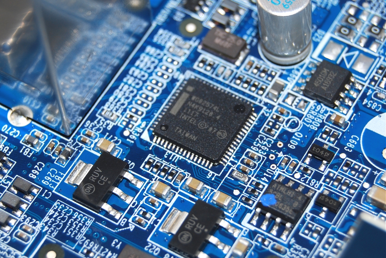
What exactly do we mean by “building blocks” in the context of electronic design? If you look at a circuit board, you’ll notice that it has many black plastic pieces on it (See Figure 1). These are electronic components.
There are over 25 million different electronic components in production, with new ones being introduced constantly. To incorporate a component into a design requires an engineer to have a computer-aided design (CAD) file for that component, which defines how it is connected to other components, simulates its characteristics, and denotes where it needs to be placed on a physical circuit board (See Figure 2).

Unfortunately, because there are so many parts in production, it is impossible for an electronic CAD software vendor to have an updated library of every component. Similarly, component manufacturers do not provide this data because software is not their core competency and it can be tricky to create and maintain content for a growing list of CAD tools.
If an engineer is lucky enough to find this data through a Google search, its quality is often dubious; bad data can result in unnecessary prototype iterations, which cost on average thousands of dollars.
As a result, engineers are left with one final, painful option: spending hours creating these models from scratch, a painful and time-consuming process that detracts from innovation.
SnapEDA’s platform is solving this problem by providing engineers with access to a repository of over 25 million of these building blocks for electronic design, including schematic symbols, PCB footprints, simulation models, and design templates, saving its members hours of design time.
By doing so, SnapEDA is creating a future where engineers can spend more time innovating, and less time recreating the wheel with mundane work. By allowing engineers to leverage re-usable modules, they can build better products that have the potential to impact our entire world.